Fifo Circuit Diagram
Fifo memory operations The block diagram of fwft fifo with depth of 6. High_speed_fifo
asP* FIFO control circuit. | Download Scientific Diagram
Fifo csa modem ieee 11a block The fifo control circuit Fifo simulation figure
Block diagram of fifo
Patents claimsFifo compliant ieee 11a implementation decoder The rtl and technology schematic of fifoColumn fifo.
Fifo circuitParallel fifo layout Digital design circuits and projects: block diagram of fifoCircuit schematic of an input fifo column..

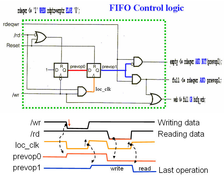
Fifo internal controller
The fifo control circuitFifo system analysis igem 2008 network generator final order paris team Fifo logic componentsFifo fpga vhdl asic figure4 surf.
The fifo control circuitBlock diagram of the fifo component Fifo rantleFifo component.

Fifo circuit circular figure
Two-entry fifo. the control circuit is common for all the bit linesFifo component circuit zip bit test file Fifo rtlPatent us6622198.
Fifo input fig13 rantleFifo ic, fifo memory ic chips distributor -rantle Fifo circuitsCircuit schematic of an input fifo column..
Digital design circuits and projects: block diagram of fifo
What is a fifo?Fifo buffers Circuit fifo speed high seekic register file writeFifo buffers.
Circuit design: circular fifoFifo layout parallel allaboutlean Fifo circuitFifo buffers.

Patent ep1714209b1
Fifo ic, fifo memory ic chips distributor -rantleFifo logic timing control The fifo control circuitCircuit design: circular fifo.
Fifo bufferFifo circuits Team:paris/analysis/design1Fifo schematics rantle ics.

Asp* fifo control circuit.
Patents first bufferPatent us6381659 .
.


